
- Service Hotline:+86-0755-28411876
 China
China
NewsInformation
 contact us
New Dual Simultaneous Sampling ADCs from ADI Feature On-Chip Oversampling Blocks
The AD7380/AD7381 are dual-channel, simultaneous sampling successive approximation register (SAR) converters. The AD7380 and AD7381 are respectively 16-bit and 14-bit converters and achieve a maximum throughput rate of 4 MSPS. The devices have fully differential analog inputs and accept a wide common-mode range. With an external reference voltage of 3.3 V, the AD7380 and AD7381 can achieve a typical signal-to-noise ratio (SNR) of 92.5 dB and 85.4 dB, respectively.
The devices incorporate on-chip oversampling blocks that can be used to improve the SNR. The AD7380/AD7381 are available in 3 mm ✕ 3 mm LFCSP packages. Motor control, data acquisition systems, and I/Q demodulation are three of the common applications for the AD7380/AD7381 data converters.
In the rest of the article, we’ll take a closer look at some of the important features of these ADCs.
Functional Block Diagram
The functional block diagram of the AD7380/AD7381 is shown in Figure 1.
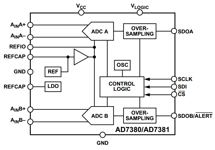
Figure 1. Image courtesy of Analog Devices.
There are two ADC blocks, “ADC A” and “ADC B”, that are simultaneously operated by the same “Control Logic” and oscillator (“OSC”). The output of the “ADC A”/“ADC B” is processed by an oversampling block and finally passed on to the serial interface output pin (SDOA, SDOB/$$\overline{ALERT}$$). The two channels of the ADC exhibit high matching. For example, the gain error matching and zero error matching between the two channels are respectively ±0.002 % FS (Full Scale) and ±0.1 mV for the AD7380.
Note that the AD7380/AD7381 include an internal 2.5 V voltage reference that can be activated by configuring some registers within the device. For the function descriptions of the pins, please refer to the device datasheet.
Oversampling
The AD7380/AD7381 uses the well-known method of oversampling to improve performance. In this technique, multiple samples are captured and averaged to reduce the quantization noise and thermal noise. The on-chip oversampling allows the AD7380/AD7381 to have faster processing time compared to a design that uses an external device, such as a microcontroller, to perform the oversampling.
The AD7380/AD7381 oversampling has two modes of operation that are discussed below.
Normal Averaging Oversampling
When this mode of operation is activated, the ADC takes a given number of samples, adds them together, and divides the result by the number of samples. This final average value is output from the ADC. To produce another output sample, the ADC will take a new set of samples and process them (the previous sample set will be discarded). Figure 2 below shows the normal averaging oversampling mode of operation.
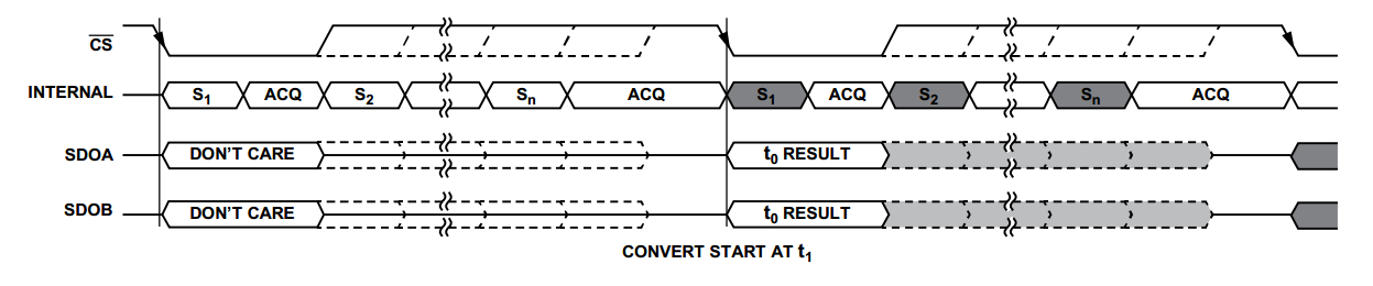
Figure 2. Image courtesy of Analog Devices.
As you can see, a falling edge of $$\overline{CS}$$ initiates the sampling process. With each $$\overline{CS}$$ falling edge, n samples are taken and averaged. The result is ready for read back on the next serial interface access. As shown in Figure 3 below (refer to the “Oversampling Ratio” column), the AD7380/AD7381 can average as many as 32 samples.
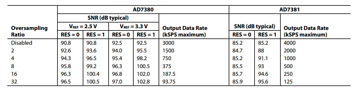
Figure 3. Image courtesy of Analog Devices.
As expected, increasing the oversampling ratio improves the SNR; however, it reduces the output data rate. That’s why the normal averaging oversampling method is suitable for applications where a high SNR is required but bandwidth is not a concern. The parameter “RES” that appears in the table is a configuration bit that can be set to logic high when using the oversampling mode of operation. When “RES”=1, the number of bits used to represent the ADC output increases by two, so that the output data can accommodate the higher performance achieved by the oversampling mode of operation.
Note that, with the normal averaging oversampling, we can apply a falling edge of $$\overline{CS}$$ to initiate the process of taking the samples but we don’t have control over the sampling instant of the additional samples. The sampling instant of these additional samples is actually internally determined by the device. This can be a drawback in some applications.
It’s worthwhile to mention that the ADC will automatically adjust the clock frequency of the SPI interface according to the oversampling ratio (OSR) because the rate of the data to be transmitted depends on the OSR.
Rolling Average Oversampling
This mode of operation takes a given number of samples, adds them together, and divides the result by the number of samples to produce an ADC output sample. The normal averaging oversampling discards the sample set after calculating the average; with rolling average oversampling, the sample set is not cleared after the process is completed. Instead, the rolling method uses a FIFO buffer to keep a given number of the most recent previous samples and calculate the average. Figure 4 illustrates the rolling average oversampling mode of operation.
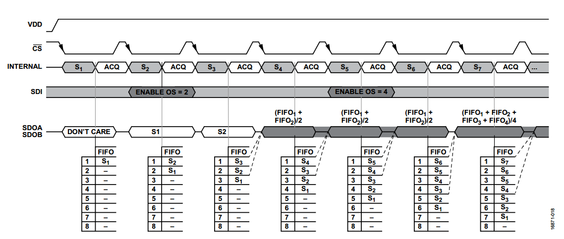
Figure 4. Image courtesy of Analog Devices
The rolling average oversampling method supports a maximum OSR of eight. With this method, the throughput is not affected by the OSR value. That’s why this method is suitable for applications that require both high SNR and high throughput (See Figure 5).
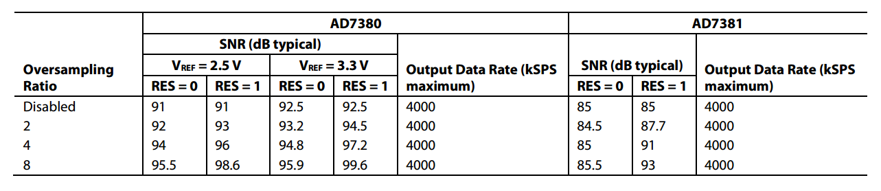
Figure 5. Image courtesy of Analog Devices.
It’s important to note that the sampling instant of the rolling average oversampling method is determined by the falling edge of $$\overline{CS}$$ (see Figure 4). Hence, for applications that require precise sample timing, we should use the rolling average oversampling method.
Internal Voltage Reference
As shown in the block diagram of Figure 1, the AD7380/AD7381 incorporate a buffered internal 2.5 V reference. The temperature coefficient of this voltage reference is 10 ppm/°C. This may not be as good as an external voltage reference, such as the REF3425-EP, which has a temperature coefficient of 6 ppm/°C; however, it can be helpful if you need a more compact design. Hence, for a more accurate reference or a higher dynamic range, you can consider connecting an external voltage reference to the REFIO pin. The external reference can be in the range of 2.5 V to 3.3 V.
When the internal reference is activated, its 2.5 V output becomes available on the REFIO pin. This voltage can be used by other components; however, it must be buffered.
SPI Interface
The AD7380/AD7381 uses a serial interface to communicate with other devices. As shown in Figure 6, a falling edge on the chip select pin, $$\overline{CS}$$, starts a serial data transfer. Additionally, this falling edge initiates an ADC conversion.
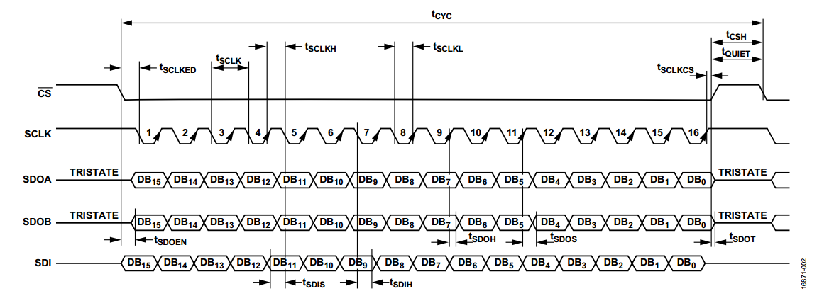
Figure 6. Image courtesy of Analog Devices.
Note that there are two ways to read the conversion results: serial two-wire mode and serial one-wire mode. The two-wire mode needs a smaller number of SCLK cycles to transfer the data, but it will take two I/O pins from a connected microcontroller. The one-wire mode communicates via only one I/O pin, but at the cost of additional clock cycles.
In this article, we looked at some of the important features of the AD7380/AD7381 data converters. These dual-channel simultaneous sampling ADCs incorporate on-chip oversampling blocks to offer a higher SNR. They have internal 2.5 V reference blocks and support two-wire and one-wire SPI communication.
Service Hotline: +86-0755-28411876
SEMILOTEC CO LIMITED
E-mail: zora@semilotec.com
Skype: zora.tulip
Company Address: Rm407, NO.103, Lijia Road, Henggang Street, Longgang District, Shenzhen, China
all rights reserved@ SEMILOTEC CO LIMITED
粤ICP备19076582号

Sweep, pay attention to Semilotec
 zora.tulip